NXP 2N7002P: A Comprehensive Overview of the Industry-Standard Small-Signal MOSFET
In the vast ecosystem of electronic components, few have achieved the ubiquitous presence and enduring relevance of the small-signal MOSFET. Among these, the NXP 2N7002P stands out as a true industry workhorse, a component that has become a default choice for designers for countless low-power switching and amplification tasks. This article provides a comprehensive overview of this fundamental device, exploring its key characteristics, internal structure, and the applications that have solidified its status.
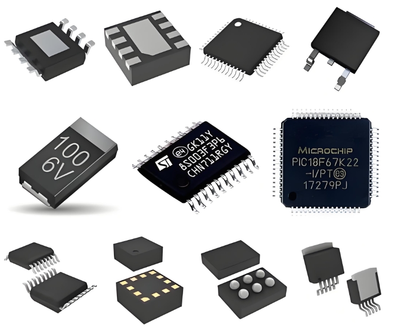
The 2N7002P is an N-channel enhancement-mode MOSFET housed in a compact, ubiquitous SOT23 surface-mount package. This package is ideal for modern, high-density PCB designs, offering a excellent balance of size and ease of handling. As an enhancement-mode device, it remains off when the gate-source voltage (V_GS) is zero. A positive voltage applied to the gate terminal relative to the source creates an electric field that forms a conductive channel, allowing current to flow between the drain and source. Its primary electrical characteristics make it exceptionally useful:
Low Threshold Voltage (V_GS(th)): Typically around 2.1V, it can be easily driven by 5V microcontroller GPIO pins and most logic families, making it a perfect interface between digital control and analog circuits.
Continuous Drain Current (I_D): With a maximum rating of 310mA, it is designed for small-signal applications such as load switching, LED driving, or signal routing, rather than power conversion.
Low On-Resistance (R_DS(on)): A sufficiently low R_DS(on) (typically 5 ohms at 10V V_GS) ensures minimal voltage drop and power loss when the switch is fully turned on, enhancing circuit efficiency.
The internal structure of the MOSFET includes an integral body-diode between the drain and source. This parasitic element is a consequence of the device's fabrication process. In circuit operation, this diode becomes forward-biased when the drain voltage falls below the source voltage, which must be considered during design, especially in inductive load scenarios where it provides a path for back-electromotive force (back-EMF).
The applications for the 2N7002P are virtually endless, underscoring its role as a fundamental building block. It is most commonly deployed as a low-side switch, where its source is connected to ground, and a microcontroller pin controls the gate to switch a load connected to the drain rail (e.g., VCC). This configuration is ideal for:
Driving DC relays, solenoids, and small motors.
Controlling LEDs and illuminating indicator lamps.
Signal multiplexing and analog switching in audio and data acquisition paths.
Implementing simple logic gates and inverters in discrete logic circuits.
Providing electrostatic discharge (ESD) protection on signal lines.
While simple to use, effective design with the 2N7002P requires attention to detail. A gate resistor (typically 100Ω) is often used to dampen ringing caused by parasitic inductance and the gate capacitance, preventing oscillation and reducing electromagnetic interference (EMI). For switching inductive loads, a flyback diode is critical to protect the MOSFET from voltage spikes generated when the current is suddenly interrupted.
ICGOODFIND: The NXP 2N7002P is far more than just a transistor; it is an indispensable component in the electronics designer's toolkit. Its perfect blend of logic-level compatibility, compact packaging, and robust performance has secured its position for decades. For any design requiring simple, efficient, and reliable low-power control, the 2N7002P remains a premier and often unbeatable choice.
Keywords: Small-Signal MOSFET, Logic-Level Gate Drive, SOT23 Package, Low-Side Switching, N-Channel Enhancement-Mode