**ADM202JRW: A Comprehensive Technical Overview and Application Guide**
The ADM202JRW stands as a quintessential example of a robust, industry-standard **RS-232 line driver/receiver** integrated circuit. This device, manufactured by Analog Devices, is engineered to facilitate serial data communication by translating logic-level signals from a Universal Asynchronous Receiver/Transmitter (UART) into the higher voltage levels required by the RS-232 standard, and vice-versa. Its design addresses the critical need for **reliable data transmission** in electrically noisy environments, making it a cornerstone component in countless industrial, telecommunications, and embedded systems.
A key technical differentiator of the ADM202JRW is its **internal charge-pump voltage converters**. Unlike older RS-232 drivers that required bulky dual power supplies (e.g., ±12V), this IC generates the necessary RS-232 voltage levels (typically between -5V and -10V for a logic '1' and +5V to +10V for a logic '0') from a single +5V power supply. This feature drastically simplifies power supply design, reduces board space, and lowers overall system cost. The device integrates four capacitors to facilitate this charge-pump operation, which are the only external components required for its basic functionality.
Furthermore, the ADM202JRW is designed for enhanced **electrostatic discharge (ESD) protection**. With ESD protection rated up to ±15 kV on its transmitter outputs and receiver inputs (using the Human Body Model), it offers superior resilience against static discharge events that commonly occur during handling or in end-user applications. This robust protection ensures a longer operational lifespan and higher field reliability, a critical factor for commercial and industrial products.
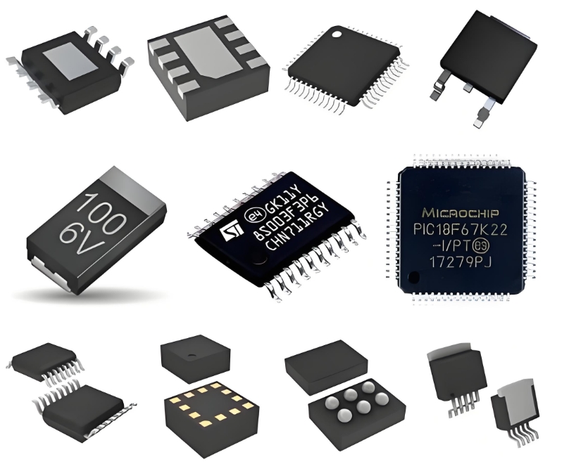
The IC features two drivers and two receivers, packaged in a compact 16-pin SOIC (Small Outline Integrated Circuit) package, denoted by the "JW" suffix. Its operational data signaling rates can reach up to **120 kbps**, making it suitable for a wide range of applications from low-speed sensor data logging to moderate-speed modem communication.
**Application Guide**
In a typical application, the ADM202JRW is placed between a microcontroller's UART pins and a DB9 or other serial port connector. The TxD (Transmit Data) pin from the microcontroller connects to a driver input (TIN) on the ADM202JRW. The driver then outputs the RS-232-compliant signal on TOUT to the connector. Conversely, the signal from an external device arrives at the receiver input (RIN), is translated down to TTL/CMOS levels, and is output on ROUT to the microcontroller's RxD (Receive Data) pin.

Design considerations include:
* **Capacitor Selection:** Use 0.1 µF capacitors as recommended by the datasheet for the charge-pump circuits. Low-ESR ceramic capacitors are ideal.
* **Layout:** Place the four charge-pump capacitors (C1 to C4) as close as possible to their respective pins on the IC to minimize parasitic inductance and ensure efficient operation.
* **Bypassing:** A standard 0.1 µF power supply decoupling capacitor should be placed near the VCC pin to ground.
* **Unused Channels:** While not mandatory, it is good practice to tie unused driver inputs to a logic high (VCC) or low (GND), and leave unused receiver outputs open.
**ICGOODFIND**
The ADM202JRW remains a highly reliable and efficient solution for modern RS-232 interface design. Its integration of key features like on-chip charge pumps and robust ESD protection into a minimal footprint provides engineers with a simple, cost-effective, and durable method for implementing serial communication, ensuring compatibility with a vast installed base of RS-232 equipment.
**Keywords:** RS-232 Transceiver, Charge-Pump Circuit, ESD Protection, Single 5V Supply, Serial Communication
